In previous articles, we explored the fundamental components of FPGA, such as Flip-Flops DFFs and Look-Up Tables LUTs. Today, we delve into the world of Configurable Logic Blocks (CLBs). Although the name may vary depending on the brand, the concept remains the same. These small arrays of configurable logic and storage elements are the building blocks of FPGA technology.
In this article, we will explore the internal organization of CLBs and how they are connected to the rest of the FPGA. We will also discuss good coding and design practices to keep in mind when working with CLBs. Finally, we will conclude by summarizing the importance of CLBs in FPGA technology and their role in digital design.
I. What is a CLB ?
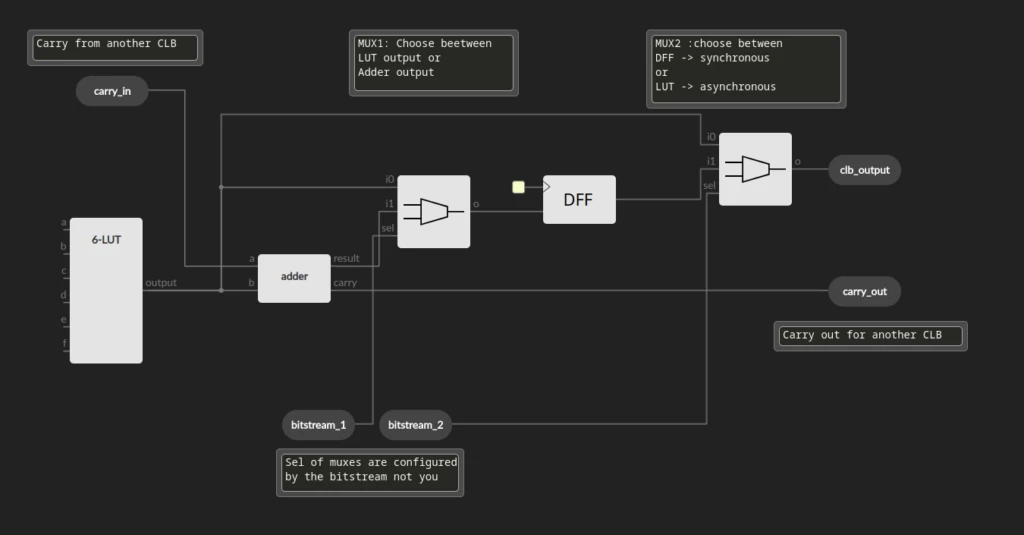
CLB stands for Creepy Little Bastard… ho sorry wrong blog … I mean Configurable Logic Block ! Which is a basic building block in FPGA. A CLB consists of LUTs, DFFs, adders and mutliplexers. Below is an architecture example of a CLB. Maybe a bad one, I did it myself, but one nonetheless. For a real one, find the architecture documentation about your FPGA.
A CLB is composed of several basic components, including a LUT for elemental combinatorial logic, a DFF to store the result of the LUT, an Adder and Carry to interconnect with other CLBs to perform large additions, and a Multiplexer to choose the output of the CLB. The LUT allows the CLB to perform various digital functions, such as AND, OR, XOR, and others, based on its input signals. The result may be stored in the DFF and can be used as a data input for subsequent operations. The Adder and Carry enable the CLB to perform large additions and carry operations, making it possible to implement complex arithmetic circuits. Finally, the Multiplexer allows the CLB to choose between multiple inputs to determine its output: from the adder, the LUT for asynchronous behavior, or the register for synchronous behavior. Giving it the flexibility to perform a wide range of functions. These components work together to make a CLB a versatile and powerful building block for digital logic design in FPGA.
The design of an FPGA’s brand architecture can vary, including differences in the number of adders and multiplexers. For example, Xilinx series 7 devices use 6-LUTs while Intel Altera devices use 8-LUTs. To ensure good design, it’s important to research and understand the specific architecture of the FPGA you’re working with.
II. How CLBs are organized within the FPGA ?
Just like other components in an FPGA, the CLB primitives are connected to the FPGA’s routing channels. These routing channels are a crucial aspect of FPGA design and deserve dedicated article…soon.
CLBs are usually grouped into larger structures such as slices in Xilinx FPGAs or ALMs in Intel Altera FPGAs. The exact composition of these structures may vary by brand, but their purpose remains the same. One important aspect of these structures is that all DFFs within them share a common clock, reset, and enable signal, which Xilinx refers to as a “Control Set”.
The management of the control sets in your design will impact the area it occupies inside your FPGA. Indeed Modules that does not share the same control set (which mean don’t have the same clock, reset, enable) cannot be instantiated in the same SLICE. If you implement a design with many control set you can end up with an FPGA where nearly all SLICE are used and nearly all those SLICE are under used. Like using the entirety of a SLICE, with several 6-LUT, registers, adders, multiplexers only to implement a AND logic function (it’s an exaggeration but the idea is here). To optimize your design, it’s important to carefully manage the number of control sets used.
III. Control Set Management
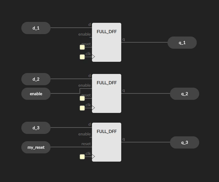
Here are three DFFs with different control set. The first only have a system clock and reset, the second has an enable, the third has a custom reset. This three DFF cannot be instantiated in the same SLICE.
Here is a way to modify your design to give them the possibility to be implemented in the same SLICE:
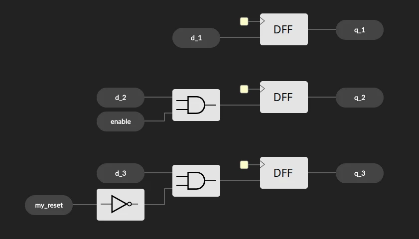
You see, here, all the DFF share the same control signal: the system clock.
Now I am asking myself: why don’t we always used this technique ? And I am not sure of the answer. My hypothesis is that we may saturate our SLICE with logic. If every signal has to be combined with a control signal, it will multiply by two the number of logic resources our FPGA needs. My other hypothesis is metastability because when you don’t know it is always metastability hahaha…. Joking aside, if you know the real answer, don’t hesitate to share it in the comment.
As with many aspects of FPGA design, it’s a matter of trade-offs. If you have too many control sets and your FPGA is becoming full, you can use the technique mentioned above. However, if you rely on it too heavily, you may encounter other issues.
Conclusion
The CLB is the basic building block in FPGAs and implements your design. It offers everything you need: logic capabilities, data storage, and connectivity with other primitives. The CLB serves as the foundation of your FPGA design. Keep in mind that the architecture of CLBs can vary between FPGA brands and generations, so it’s important to familiarize yourself with the architecture by reading the relevant documentation.
I hope this article gave you a clearer understanding of how FPGAs work. If you found it helpful, please consider bookmarking this blog, sharing the article, and leaving a comment. Thank you for reading!