DFF stand for D Flip-Flop. It is one of the most important pieces of circuitry of your FPGA.
This hardware primitive allow you to store the smallest amount of memory in your FPGA, 1 bit, 0 or 1.
It is as important as variables in a software code. Ask a software developer what he/she can do without variables…
That’s why I think it is a good start to have a deep understanding of what DFF is if you are a beginner.
Even if you change of FPGA’s brand, DFFs are quite all the same. For intellectual property reason, or just to be different, every brand will call its DFF, the inputs/outputs of DFF or the structure containing the DFF with different names. These changes of name often occurred so better be aware that things you have on one FPGA will be called differently on another FPGA from a different brand.
In this article we will see the Inputs and Outputs of the DFF and their purpose, then we will focus on their location inside the FPGA, some timing notion and finally code example in VHDL and Verilog.
Inputs and Outputs of a DFF
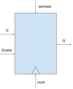
DFF has several inputs/outputs : clock, reset, enable, d, q.
1.D: the input signal, d can stand either for “Data” or “Delay”. It is the signal that you want to memorize the state of.
2.Enable : input control signal, usually active high meaning that when asserted (enablee=1) the D input state is transferred to the Q output on the clock tick. When not asserted (enable=0) Q keep its value of the last clock tick, without considering the value of the D input. If you don’t use the “enable” in your code, the synthesizer will put the “enable” signal to 1.
3.Reset : input control signal, commonly called reset and active high, when asserted, it will set the Q value to the Reset value that you have indicated in your design code (see code examples below). The reset can be synchronous, meaning Q will change only after the clock tick. Or asynchronous, meaning that Q will take the reset value as soon as possible.
4.Clock : which deserve an article all by itself if not more. The clock is a square signal input that will tick at a precise frequency. It dictates when, and for how long, a change will occur on the output Q of the DFF, if change there is, and if the change is synchronous.
5.Q : the output of the DFF, which will have a value that depends on all the control signal and data signal above. You can sometimes find a second output which is the inverted value of Q.
For an active high reset and an active high enable the truth table is the following:
| value of reset at cycle n | value of enable at cycle n | value of q at cycle n+1 |
|---|---|---|
| 1 | X* | reset value |
| 0 | 1 | the value of d at cycle n |
| 0 | 0 | the value of q at cycle n last time enable was 1 |
*Here ‘X’ mean whatever 0 or 1.
Where are the DFFs inside of an FPGA ?
Usually DFF in FPGAs are included in a bigger structure (SLICE for xilinx, ALM for Altera). You will find several DFF in such a structure that share the same control signals. Sixteen DFFs per slice in xilinx ultrascale and only 8 in series 7 FPGA. Two or four in for ALM of Altera. This bigger structures contain other elements like LUTs but we will keep it simple for the moment.
I did not find any information on this topic, but my guess is that DFF have the same control signal inside SLICE or ALM to reduce the number of wire inside the FPGA.
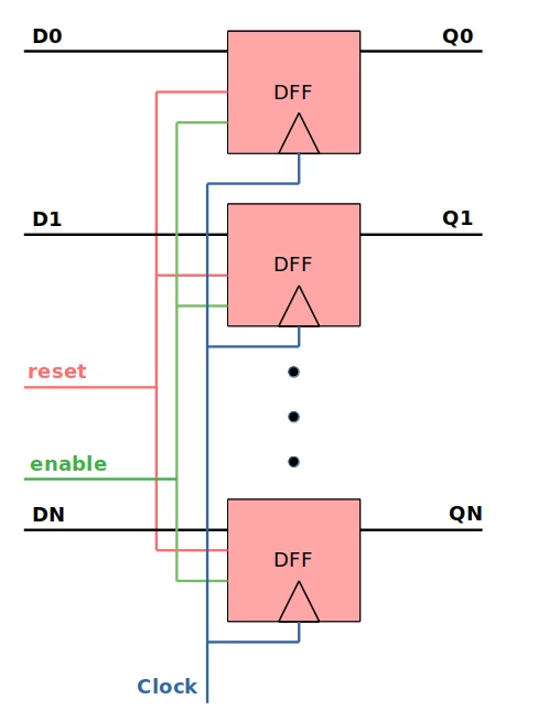
The fact that DFFs in a SLICE/ALM have all the same clock, reset and enable implies that two signals d that are controlled by a different set of clock, reset and enable will be instantiated on two DFFs that are not on the same SLICE/ALM. In consequence, the more you have different control set (clock, reset, enable) in your design, the more your FPGA will be filled with half-full SLICE/ALM. Meaning waste of resources. We will see how to bypass this problem in a future article.
Timing notions
The behavior presented above is true in a perfect mathematical world but in reality some constraints must be met for the DFF to work as expected. These constraints are timing.
Indeed the value of d has to be held for a certain period of time before and after the clock tick occurred so that the value of input d is copied by the output q.
Those two durations are called:
Setup Time: the minimum amount of time that the value of D has to be held BEFORE the clock tick.
Hold Time: the minimum amount of time that the value of D has to be held AFTER the clock tick.
Aperture = Setup Time + Hold Time
In case of an asynchronous reset the DFF copy the Reset value to Q, not the value of D and regardless of the clock tick occurring. There should be a minimum amount of time before and after the de-assertion of the reset signal so that the DFF goes back to copying the value of D in Q on the clock tick. These times are called :
Recovery Time: the minimum amount of time the reset must be de-asserted BEFORE the clock tick occurred, to allow the DFF to reliably copy D in Q on the clock tick.
Removal Time: the minimum amount of time the reset must be de-asserted AFTER the clock tick occurred, to allow the DFF to reliably copy D in Q on the clock tick.
Interviewers really like to ask the definition and explanation of those 5 terms, so better learn them now 😉
Code examples DFF
DFF without control signals
Here is the code example of a DFF in Verilog and VHDL. If you want code examples of DFF without “enable” or “reset”, with synchronous reset or asynchronous reset you can go on the blog GitHub here
In Verilog:
module dff(
    input clock,
    input d,
    input reset,
    input enable,
    output reg q
);

always @(posedge clock)
begin
    if(reset)
        q <= 1'b0;
    else
        if(enable)
            q <= d;
end
endmodule
In VHDL:
library ieee;
use ieee.std_logic_1164.all;

entity dff is
port (
    d      : in std_logic;
    clock  : in std_logic;
    reset  : in std_logic;
    enable : in std_logic;
    q      : out std_logic
);
end entity;

architecture arch of dff is

begin

ps_dff : process(clock)
begin
    if (rising_edge(clock)) then
        if (reset='1') then
            q <= '0';
        elsif(enable='1') then
            q <= d;
        end if;
    end if;
end process;

end architecture;
Conclusion
Knowing how DFF works is fundamental for your understanding of FPGA. You will use it every day during your FPGA career. Your next employer will ask you some of the information above without a doubt.
If you have any question about DFF please post a comment here, I will answer. If you see any error or an oversight please post a comment too. And otherwise comment ! I will be happy to read it (preferably post insult on Twitter :p ).