When I was a child, the back of my cathodic TV amazed me. I wondered what were all those cables and what were their purposes. I learned that it was electricity after. Then that it was only 0 and 1. And I couldn’t stop asking myself, “how can we do anything with only 0 and 1?”
If you asked yourself this question, you’re in the right place. Because today is the day we speak about combinational logic and LUTs. Of course combinational logic and LUTs aren’t the only way to process a signal in electronic, but it’s a tiny part that could have satisfied my curiosity back then. And it’s a huge part of how FPGA does it.
In a previous article about DFF, we saw how to store data in our FPGA. Today it’s time to study how to manipulate those data. First we will learn about logic gates, how they work and how it’s absolutely not what is implemented in an FPGA, and why LUT is used instead.
1. What is a logic gate ?
Logic gates are hardware implementation of the bitwise operations you can do with 1 or 2 bits. They’re the different operation you can do in Boolean algebra.
With one bit you don’t really have the choice, you can :
- do nothing which is … not a gate, it’s a wire.
- invert the bit. If it’s a 1, it becomes a 0. If it’s a 0, it becomes a 1.
For a gate with two inputs bit and only one output bit, we can use:
- The AND gate. The output is a 1, if and only if both input bits are 1.
- The OR gate. The output is a 1, if at least one of the two input bits is 1.
- The XOR gate (eXclusive OR). The output is 1 if and only if one of the inputs is 1 (the other one must be 0)
– And that’s it !
– Wait ! I heard there are seven logic gates. You showed only four of them !
Yes, the three missing gates are the NAND, the NOR and the XNOR which are just the three above with and inverters on the output.
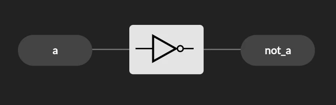
1.1 The inverter
The symbol of the inverter. Notice the little circle at the end of the triangle ? This is the symbol of “not” you will find it in NAND, NOR, XNOR too.
| a | not a |
| 0 | 1 |
| 1 | 0 |
1.2 AND gate
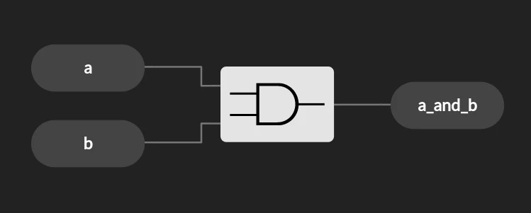
| a | b | a AND b |
| 0 | 0 | 0 |
| 0 | 1 | 0 |
| 1 | 0 | 0 |
| 1 | 1 | 1 |
1.3 NAND gate
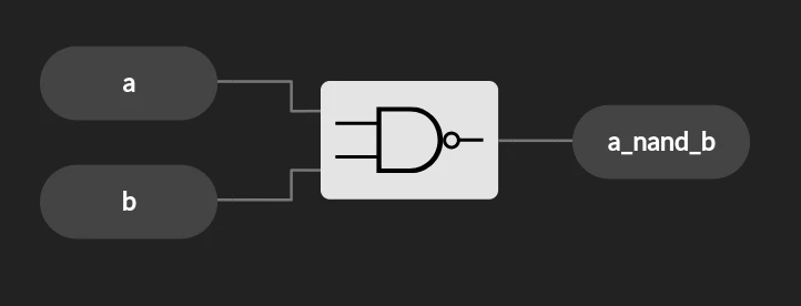
| a | b | a NAND b |
| 0 | 0 | 1 |
| 0 | 1 | 1 |
| 1 | 0 | 1 |
| 1 | 1 | 0 |
1.4 OR gate
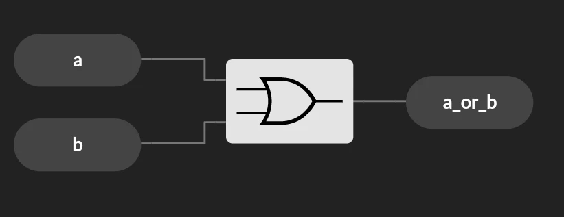
| a | b | a OR b |
| 0 | 0 | 0 |
| 0 | 1 | 1 |
| 1 | 0 | 1 |
| 1 | 1 | 1 |
1.5 NOR gate
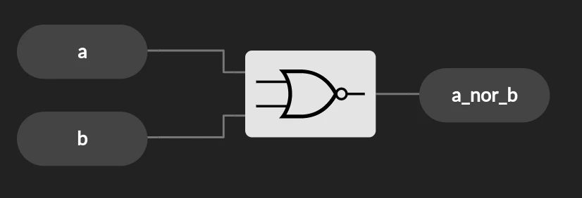
| a | b | a NOR b |
| 0 | 0 | 1 |
| 0 | 1 | 0 |
| 1 | 0 | 0 |
| 1 | 1 | 0 |
1.6 XOR gate
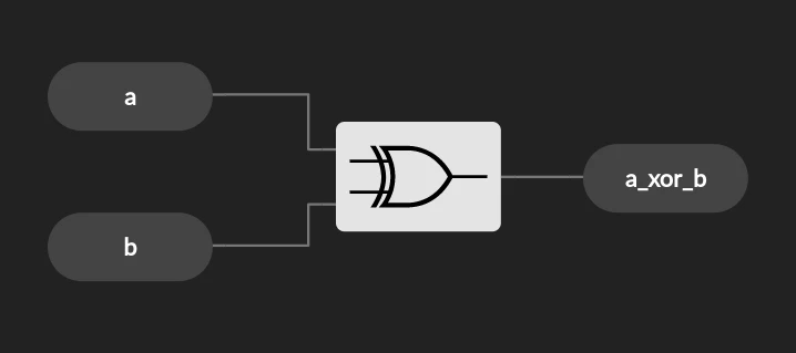
| a | b | a XOR b |
| 0 | 0 | 0 |
| 0 | 1 | 1 |
| 1 | 0 | 1 |
| 1 | 1 | 0 |
1.7 XNOR gate
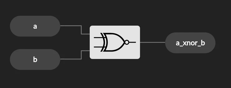
| a | b | a XNOR b |
| 0 | 0 | 1 |
| 0 | 1 | 0 |
| 1 | 0 | 0 |
| 1 | 1 | 1 |
2. Example : The adder.
Let’s see one of the most simple designs we can do with those gates : the adder. We have two inputs bits and want to add them together.
Given two bits “a” and “b”, then a+b<=2. Since 2 is written “10” in binary, we need two outputs, one for each binary figure.
Knowing the result of the right figure is equivalent to ask : when does the addition’s result is equal to 1 ? If one of the two bits is equal to 1 but not both which is… a XOR gate that’s right.
When does the second figure is equal to 1 = when does the result is equal to 2 ? If both of the bits are 1 which is… a AND gate.
That’s it ! you made an adder:
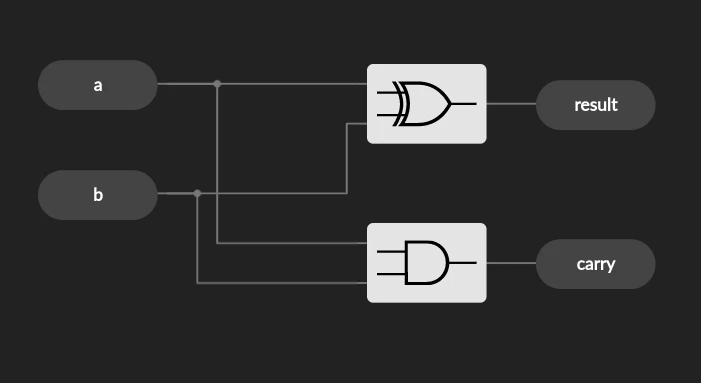
Since we had to create another figure to represent the 2 in binary, the second figure is called the “carry” in the same way we have carries in decimal addition. “result” is the right figure. “carry” is the left figure of the addition.
At this point we could think that our FPGA is full of AND, OR, XOR gates which implement our design. This is actually not how it works and it’s the topic of our next part.
3. What is a LUT ?
LUT stands for Look Up Table. It is the hardware instance of a reconfigurable truth table, which can describe any boolean equation of N variables.
A LUT is instantiated as cascading multiplexers of two inputs and one output. The two inputs are SRAM configured during the power up of your FPGA. Your boolean variables are the “select” input of the multiplexer.
A 3-LUT can be represented like this (is it not how they are design in silicon) :
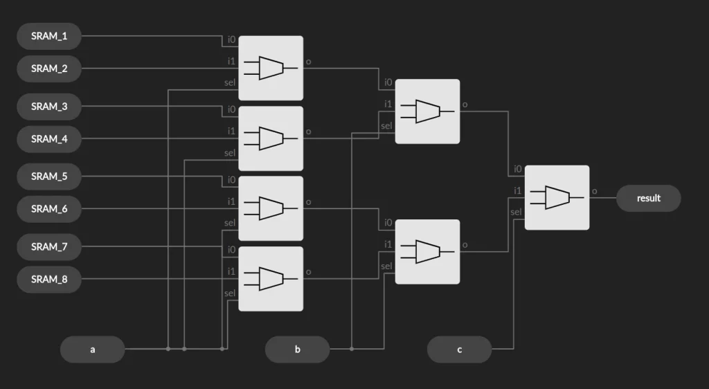
Any boolean equation with three variables can be instantiated with this 3-LUT. To change the equation we just need to change the value inside the SRAMs. I say “we” but it is actually the synthesizer and “place and route” tools who are going to configure the LUTs. The picture of the 3-LUT above is made with IceStudio, but you will never have to instantiate a LUT by hand. I made it purely for educational purpose.
Here is an example of how a LUT could be configured for a XOR and a AND gate inside an FPGA:
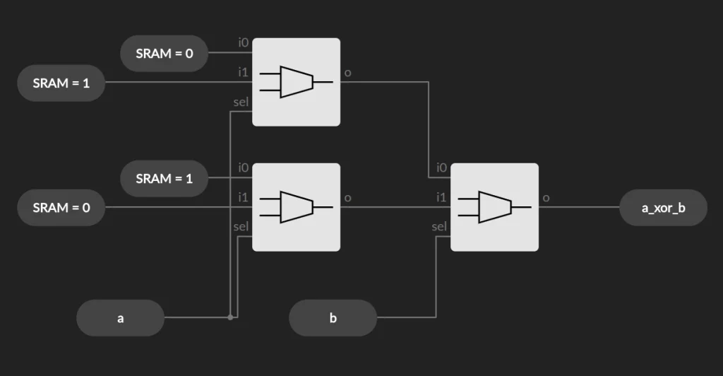
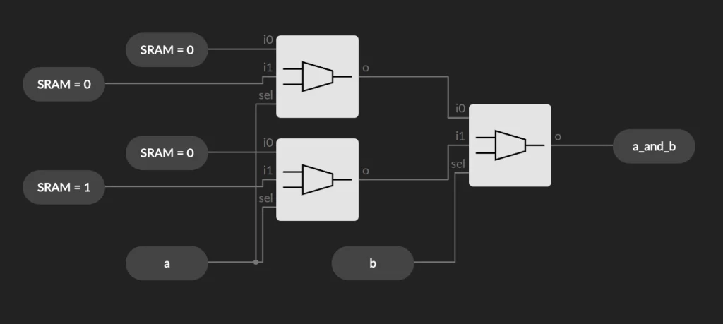
You see ? We only need to change the SRAM value to change the operation. With a 2-LUT you can reproduce all the gates described above. And with a N-LUT, any equation with N variables.
FPGA contains thousands of LUTs that will allow you to implement very complex designs.
The number of inputs and outputs of a LUT can vary depending on the constructor and the version of your FPGA. For example, the Xilinx 7 serie got 6-LUT that can be configured as two 5-LUT as long as the 5 variables are the same, whereas the Altera ones got 8-LUT that can be configured as a 3-LUT + a 5-LUT (and many other configurations). When you work on FPGA, it is always good to know what architecture the constructor have chosen. Xilinx also give you coding style advice next to the architecture presentation so you can take advantage of the full potential of their FPGA.
Conclusion
Now, you know how combinational logic works in FPGA and with my previous article on DFF you now know the two most important piece of circuitry in your FPGA.
Again, it’s important that you know what is instantiated with your code !
If you like the blog or post, don’t forget to share it, bookmark it and to comment it 🙂
Hope you enjoyed !


One Response
This is elementary circuiting, but the bases are important, because if we don’t get them right, nothing further can be understood.
Thank you four your effort to explain them clearly and simply.